last version: 24/04/2024
01. Motherboard, CPU and Address Space
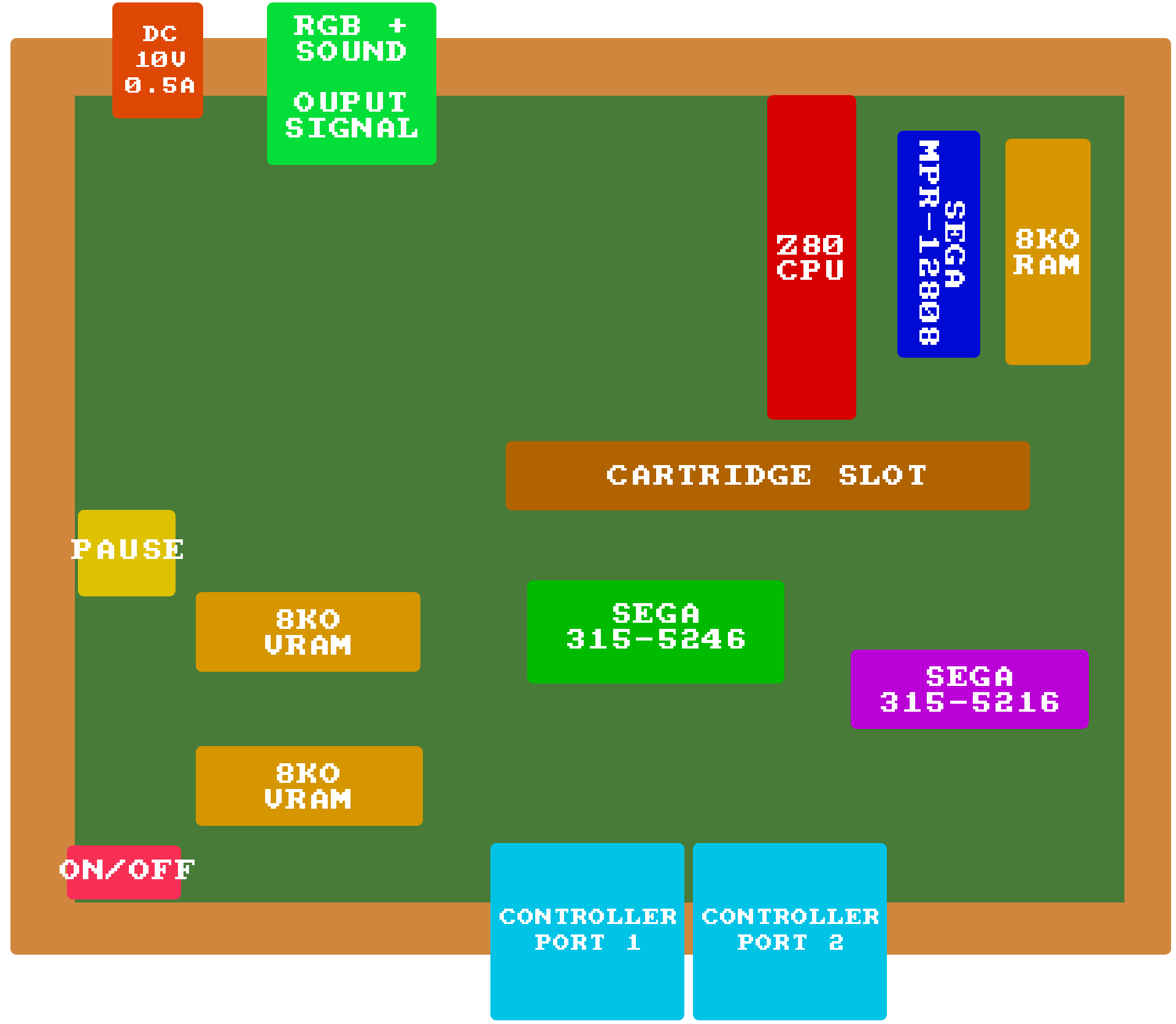
Motherboard
The motherboard of the Sega Master System 2 (Europe version) looks like this:
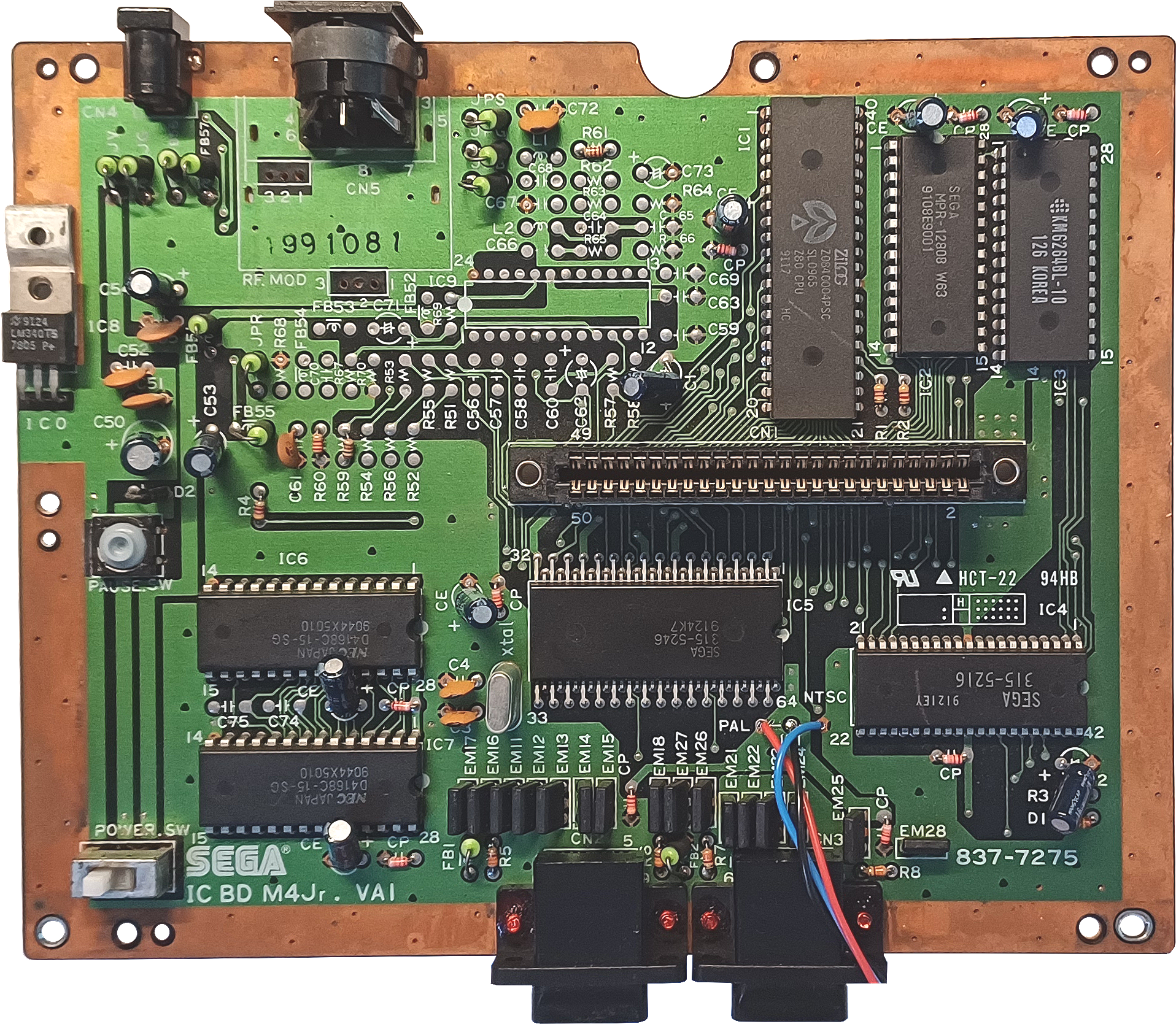
The three cables (red, black and blue) are not here by default. I welded them together for switching from PAL to NTSC region.
The specificity of the European version is the RGB output signal that which replaces the version with RF video output.
Its components (for the Sega Master System II) are:
- CPU: Zilog Z80.
- RAM: 8Ko (Samsung KM6264BL-10).
- ROM: Sega MPR-12808 chip that contains the BIOS program and the game 'Alex Kidd'.
- VDP and PSG: Sega 315-5246 chip that contains the Video Display Processor derived from the Texas Instruments TMS9918, and the Programmable Sound Generators SN76489.
- VRAM: 16Ko (from 2 chips NEC D4168C-15-SG).
- I/O Controller: Sega 315-5216.
- 2x DB9 Controller port.
Cartridge
The content of a cartridge looks like this (without any ROM mapper, or SRAM for saves):
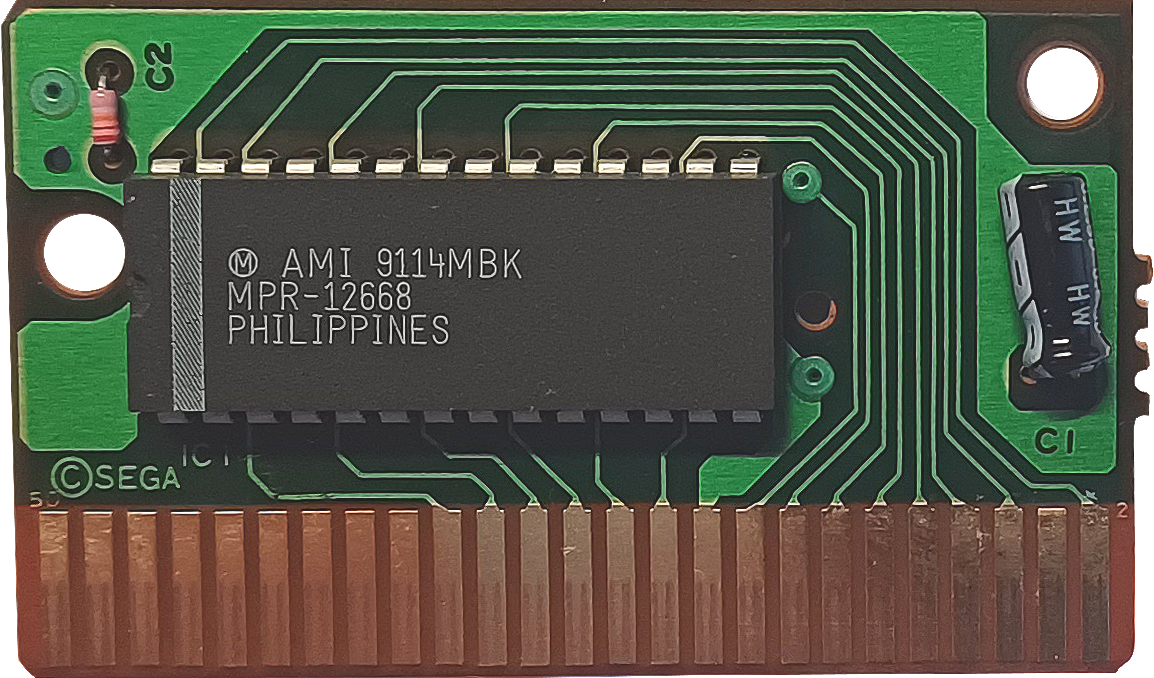
This chip MPR-12668 contains the ROM 'SMS Teddy Boy (EU)', for more information about chip numbers, see ROMPartNumbers.
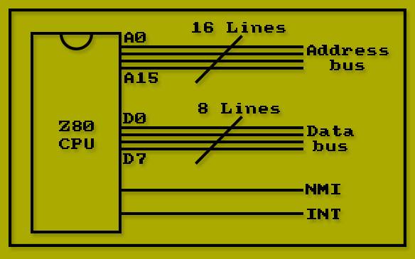
CPU - Zilog Z80
This 8-bit microprocessor was very popular in the 80's and was used in many computers and arcade games:
- ZX Spectrum.
- Game Boy (and it's variants: Game Boy Color, Game Boy Advance (as a secondary microprocessor)).
- Sega Genesis (as a secondary microprocessor).
- Arcade PacMan.
- Arcade Donkey Kong.
- other.
Today, it still can be found on some electronic boards and retro-computer projects, but it's no longer a component used on a daily basis.
The 15th April 2024, Zilog have announced the end of production for this processor.
This microprocessor is made up of:
- Address Bus (output): 16 lines from A0 to A15.
- Data Bus (input/output): 8 lines from D0 to D7.
- INT: Interrupt Request generated by I/O devices.
- NMI: Nonmaskable Interrupt (where the pause button is connected).
- other pins that will not be covered here.
For more information about how this microprocessor works, see Wikipedia.
The official Z80 documentation is here: Z80 user manual
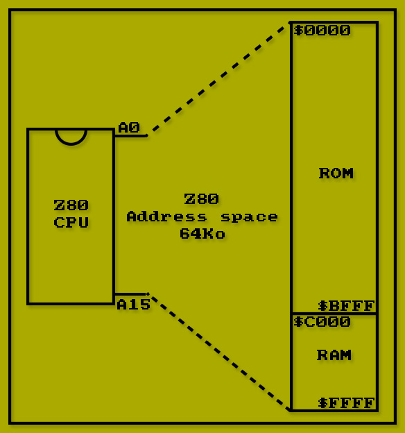
CPU - Address space
The Z80 has 16 pins devoted for address bus and each one can be ether a one or a zero. So, we have 2^16 = 65536 different memory addresses, noted in hexadecimal from $0000 for the first address to $FFFF for the last one, that can be accessed by the CPU.
So, we call Address space all the differents addresses that the CPU can reached within the Address Bus pins, regardless of whether these addresses corresponds to a location in a ROM or RAM chip.
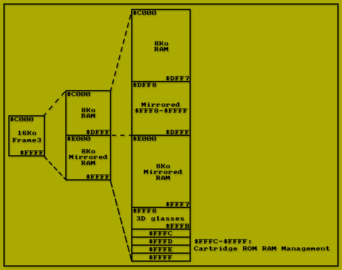
On the Sega Master System, these 64Ko addresses are split like that:
- 48Ko for the ROM.
- 16Ko for the RAM (8Ko for the RAM only, and the remainder are Mirrored RAM).
But why it's like that ?
This kind of configuration is not mandatory (if you want to build your own game console). You can choose, for example, to have half of the address space dedicated for ROM and the remaining half for the RAM. This configuration is determined when the circuit is drawn by engineers.
For a home console, we doesn't need to store many data in RAM, but we need to access a lot of data from the cartridge itself.
What's more, the RAM, at the time, was expensive. So, if you want to be in a within acceptable prices, you need to reduce characteristics like the RAM.
How does the CPU knows which component is ROM or RAM ?
The answer: it doesn't know at all. But the programmer does !
This configuration derives from the way the chips are connected to each other.
In our address space, we see that addresses below $C000 are for the ROM, and above (including itself) for the RAM. So, let's check it out the Address bus lines to understand what's going on:
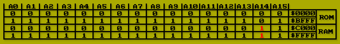
As we can see, pin A14 is the only one that determines whether we want to talk to the ROM or RAM chip.
All addresses, between $0000 to $BFFF, that map the ROM, have A14 at 0. But all addresses, between $C000 to $FFFF, that map the RAM, have A14 at 1.
So, we can used pin A14 to determine which chip is active or not:
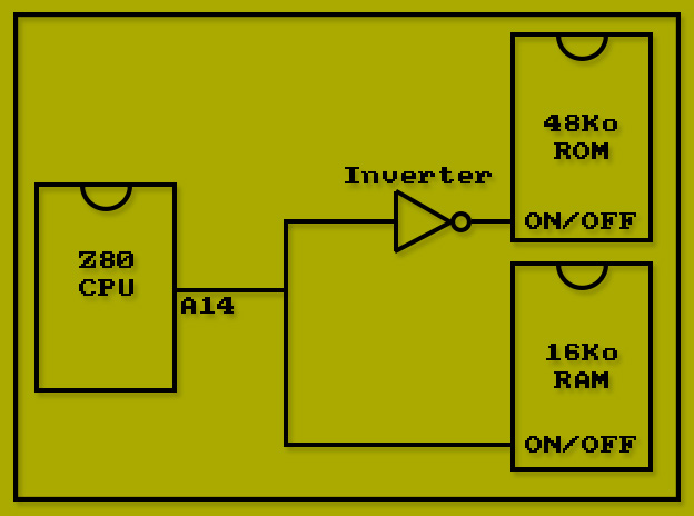
The inverter inverse the value of A14. At 0, the value become 1 to enable the chip.
This is an example, this diagram doesn't exactly represent the actual connection on the motherboard. There is a Memory Decoder chip, embedded in the Sega 315-5216 I/O Controller, which controls which chip is active at a given time.
You can check 'Understanding the Z80 Memory Map' from Kenneth Finnegan.
ROM Addresses
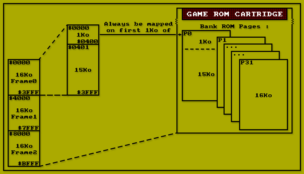
These 48Ko of memory addresses are divided into 3 chunks of 16ko each, named Frame0 to Frame2.
It's from these addresses that we can read data (software, sprites, tiles, musics) directly from the cartridge.
So, if we try to read a value, between $0000 to $BFFF, we read directly from the cartridge.
In the cartridge, all data are organised in 16Ko pages, from page 0 to page 31.
For the Frame0, the first 1Ko is always mapped to the first 1Ko in the cartridge.
For the remaining 15Ko of Frame0, Frame1 and Frame2, we can swap which pages, from the cartridge, we want to read.
Swapping pages will be a dedicated chapter.
RAM Addresses
The last remaining 16Ko of memory addresses, named Frame3, are divided into several sections:
- from $C000 to $DFF7, this is the 8Ko RAM (minus 8 bytes) used by the CPU.
- from $DFF8 to $DFFF, here are all mirrored values from $FFFC to $FFFF
- from $E000 to $FFF7, here are all mirrored value from the RAM.
- from $FFFC to $FFFF, this 4 bytes are used for swapping pages in the cardrige.
What's Mirrored RAM ?
It was something that didn't make sense to me and I think it's good to take a few lines to understand.
So, as we have seen, there is 16 lines in the Z80 cpu, from A0 to A15, for address bus.
In the meantime, the 8Ko of RAM (from Samsung KM6264BL-10) has only 13 pins, from A0 to A12, for addressing all the memory.
The pins of these two components A0 to A12 are connected together (the A0 from Z80 is connected to the A0 from the Samsung chip, and so on).
So, A13, A14 and A15 are not used to decrypt the RAM address.
For example: reading a byte from $C42B or $E42B, without A13 to A15, gives the same values from A0 through A12.

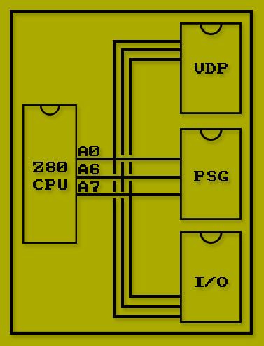
I/O devices
The Z80 CPU can communicate with external devices (keyboard, screen, joypad) via the first 8 pins address bus (A0 to A7). On the Sega Master System, the pins A0, A6 and A7 are used to communicate with these external devices :
- $BE and $BF: the VDP chip.
- $DC and $DD: the I/O Controller chip.
- $7E and $7F: the PSG chip.
- $3E and $3F: the Memory Control chip.
We will see later at how to communicate and transfer data with these devices. But you can check SMS/GG hardware notes by Charles MacDonald, for more informations about I/O addresses.